


TL;DR
- Evaluation of engineering partners requires verifying their mastery of high-speed digital architectures and embedded hardware-firmware integration.
- Experienced engineering partners like Conclusive Engineering embed Design for Manufacturability (DFM)principles early to reduce costly assembly defects and material waste.
- Hardware firms must hold relevant ISO certifications and perform pre-compliance testing to secure UKCA and CE approvals seamlessly.
- Proactive supply chain management utilises defensive dual-footprint layouts to mitigate component obsolescenceand maintain production schedules.
The selection of Electronic Design Services (EDS) requires a systematic review of an engineering partner’s technical competencies, design methodologies, and supply chain controls. In this guide, you will learn how to assess external engineering teams that develop custom hardware, printed circuit boards (PCBs), and embedded systems. You must verify that your chosen partner translates complex system architectures into production-ready physical devices. The evaluation ensures the firm can proactively mitigate electromagnetic interference (EMI) and component obsolescence risks.
Evaluation of Core Engineering and Technical Competencies
The evaluation of an electronic design firm’s core technical capabilities requires verifying their mastery of high-speed digital architectures, RF integration, advanced ECAD tools, and embedded hardware-firmware co-design. Such verification ensures the chosen partner possesses the specific engineering depth necessary for your product sector.
ECAD Platform Mastery and Advanced PCB Architectures
High-tier engineering firms operate using industry-standard Electronic Computer-Aided Design (ECAD) software platforms. Programs such as Altium Designer and Cadence Allegro handle massive multi-layer routing, complex thermal simulations, and dense board topographies.
Open-source suites like KiCad provide excellent flexibility for rapid prototyping and medium-complexity designs. The engineering team must demonstrate experience designing specialised physical board types to fit the product enclosure envelope. Such architectures include High-Density Interconnect (HDI), rigid-flex boards, and metal-core PCBs (MCPCB).
Advanced designers must also integrate their 2D electrical layouts tightly with 3D mechanical CAD tools like SolidWorks. This integration ensures precise, collision-free enclosure fitting before physical prototypes are ordered.
Signal Integrity, RF, and Thermal Management
Design partners must prove their ability to manage complex high-speed signal integrity challenges to prevent critical data loss. Engineers implement controlled impedance routing and precise differential pair matching for fast microprocessors and Radio Frequency (RF) communication modules. This mastery ensures reliable, uninterrupted Wi-Fi, Bluetooth, or cellular data transmission without harmful signal reflection.
They also incorporate dedicated, robust thermal management strategies directly into the initial PCB layout phase. Advanced techniques like custom thermal vias, optimised copper pours, and heat sink integrations dissipate intense energy effectively.
Embedded Firmware Integration
Comprehensive design providers employ internal firmware engineering teams to facilitate seamless hardware-firmware co-design. These specialists tightly couple the physical hardware architecture with low-level software execution for maximum device efficiency.
They must be highly proficient in both lean bare-metal programming and complex Real-Time Operating Systems (RTOS) architectures. Bare-metal code maximises speed for simple microcontrollers, whereas RTOS manages multiple concurrent tasks for complex processing units.
Evaluation of Design for Excellence (DfX) and Manufacturing Readiness
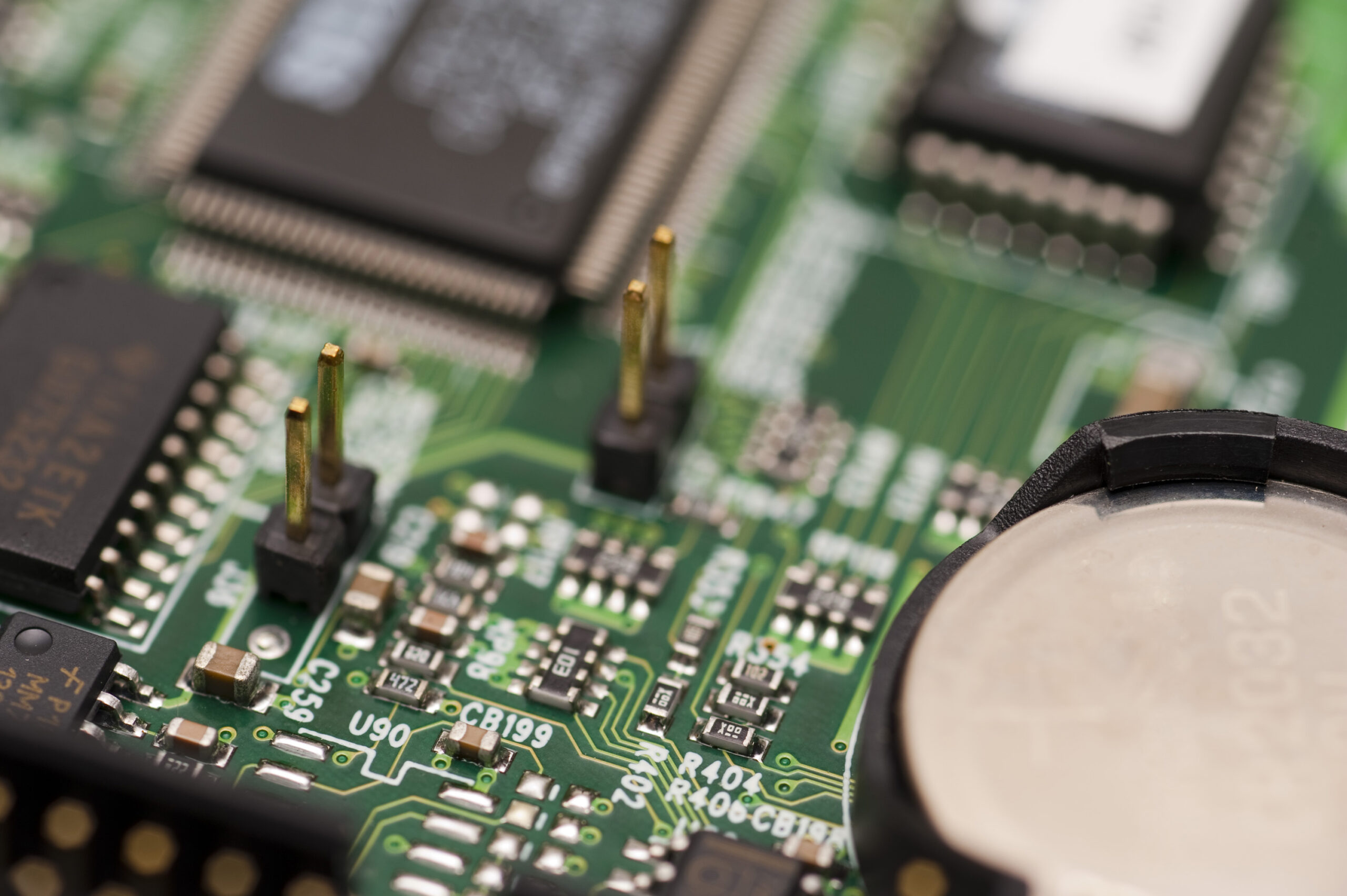
Image by stockmedia.cc
A design firm proves its manufacturing readiness by embedding Design for Excellence (DfX) principles directly into early schematic capture and board layout. High-end partners, such as Conclusive Engineering, deliver end-to-end custom electronic design services that bridge the gap between initial prototyping and scalable volume production.
Design for Manufacturability (DFM) and Assembly (DFA)
Designers must account for the strict physical constraints of fabrication facilities during the initial layout phase. This Design for Manufacturability (DFM) process requires setting appropriate minimum trace widths, copper clearance boundaries, and precise annular ring sizes. Engineers also implement optimized panelisation strategies across the layout.
Effective Design for Assembly (DFA) further optimises the board geometry for automated Pick-and-Place machines. Teams must align and space components correctly to accommodate distinct manufacturing operations, such as wave soldering versus reflow soldering.
These proactive layout choices mitigate severe manufacturing defects that ruin batches of boards. Correct spacing prevents issues like tombstoning, unwanted solder bridges, and thermal shadowing.
Design for Testing (DFT)
A rigorous hardware design process must incorporate structural testability directly into the PCB architecture. Engineers place accessible physical test points throughout the board layout to enable rapid electronic evaluation. These specific nodes allow assembly lines to utilize high-throughput In-Circuit Testing (ICT) or Flying Probe testing equipment during mass production.
Designers also integrate specialized boundary-scan architectures, such as the JTAG standard, into the board’s design logic. This digital infrastructure allows automated factory systems to verify intricate chip interconnects and program embedded microcontrollers directly on the line. The technique functions without relying on external physical probes touching fragile fine-pitch components.
Assurance of Quality Standards, Compliance, and Certifications
Regulatory and quality verification requires selecting a design partner that adheres to strict IPC standards, maintains robust Quality Management Systems, and executes pre-compliance testing. This stringent vetting ensures the final hardware meets all regional legal and safety obligations.
Adherence to IPC Standards and Quality Management Systems
Professional design services construct their layouts to strictly meet Institute of Printed Circuits (IPC) global acceptability standards. The firm must understand the distinction between bare board acceptability (IPC-A-600) and final populated assembly standards (IPC-A-610).
Buyers must specify if their product requires standard IPC Class 2 design for dedicated service or demanding IPC Class 3 design for high-reliability aerospace components. Top-tier providers also maintain active ISO 9001 certifications to ensure consistent quality management and process control throughout the hardware lifecycle.
Specialized markets demand even stricter regulatory compliance standards from engineering partners. Hardware firms must hold an ISO 13485 certification to legally develop products for the regulated medical device sector, governed in the UK by the MHRA.
Pre-Compliance Testing and UKCA Certification
Effective partners embed proactive regulatory compliance strategies directly into the early PCB layout phase. Engineers apply proper grounding planes, strategic decoupling capacitors, and shielding cans over noisy RF components to mitigate Electromagnetic Interference (EMI).
The firm should possess internal laboratory equipment like near-field probes and spectrum analyzers to perform in-house pre-compliance testing. This testing ensures the final device easily passes official CE or UKCA marking assessment for the UK market on the first attempt. While the CE mark is recognized in the UK for most electronics, early compliance testing remains essential for either standard.
Management of Supply Chain Risks and Intellectual Property

Long-term commercial viability depends on evaluating a vendor’s supply chain intelligence, obsolescence management, and legal IP protection practices. A rigorous evaluation prevents unforeseen manufacturing blockages and secures your proprietary designs.
Component Obsolescence and Alternate Sourcing Strategies
Supply chain resilience begins long before any physical manufacturing commences on the factory floor. High-quality engineering partners continuously monitor the Bill of Materials (BOM) during schematic capture using specialized supply chain software. Tools like SiliconExpert or Octopart provide live inventory metrics.
This vigilance identifies specific components approaching End of Life (EOL) or Not Recommended for New Design (NRND) statuses immediately. To mitigate future supply chain disruption, the firm actively designs defensive layout footprints using standard component packages.
Engineers also deploy dual-footprint design strategies for critical silicon chips. These clever layouts allow the board to accept multiple physically different, but functionally identical, microcontrollers depending on real-time market stock availability.
Intellectual Property Ownership and Data Security
Design outsourcing inherently requires sharing highly sensitive technological concepts and trade secrets with a third party. Both entities must execute strict mutual Non-Disclosure Agreements (NDAs) before discussing any specific product requirements or system architectures.
The final Master Services Agreement (MSA) must establish clear Intellectual Property (IP) ownership structures defined exclusively as a “Work for Hire” arrangement. This vital contract secures the client’s full and unencumbered legal rights to all generated schematics, manufacturing files, and firmware source code upon final payment.
Furthermore, the partner must utilise secure, heavily access-controlled data environments. This security protects these critical design assets from unauthorised extraction or external cyber threats often found on consumer-grade cloud storage platforms.
Handover of Project Deliverables and Essential Contract Terms
A comprehensive electronic design engagement must conclude with complete, unencumbered handoffs of all native production, manufacturing, and software assets. The final project package must include the native ECAD source files alongside all corresponding manufacturing exports.
These production files consist of standard Gerber formats (RS-274X or X2) or ODB++ files, NC Drill files, and Centroid data files used for automated assembly machines. The vendor must provide a fully scrubbed, optimized Bill of Materials (BOM) spreadsheet detailing exact manufacturer part numbers and approved alternates.
Buyers should also receive the complete firmware source code, compiled binaries, and formal Statement of Work (SOW) documentation. This paperwork confirms all Engineering Validation Testing (EVT) and Design Validation Testing (DVT) milestones.
Frequently Asked Questions
What is the difference between a PCB design service and a turnkey electronics manufacturer?
A PCB design service strictly generates engineering logic and files. A turnkey manufacturer provides those design services while also procuring components and assembling the physical boards. A turnkey model consolidates vendor management but often limits your flexibility to migrate mass production to alternative fabrication facilities later.
What files should an electronics design firm deliver at the end of a project?
Firms must provide native ECAD layouts, standard manufacturing exports like Gerbers or ODB++, NC Drill files, and a scrubbed BOM spreadsheet. Full ownership of these native source files allows you to switch engineering partners later without starting the schematic design from scratch.
How do engineering firms handle component shortages and obsolescence?
Engineers perform BOM lifecycle analyses using software like SiliconExpert to identify End-of-Life parts and design defensive, dual-footprint layouts for drop-in replacements. This proactive identification prevents costly mid-production board re-spins that can delay your market launch.
How do electronics design services ensure a product passes UKCA and CE certification?
They incorporate strict EMI/EMC mitigation strategies directly into the PCB layout and perform localized pre-compliance testing using near-field probes. This early testing prevents official certification failures, which can cause significant delays in market launch.
What quality certifications should a medical device hardware partner hold in the UK?
Medical device engineering firms must hold an active ISO 13485 certification and demonstrate strict adherence to the MHRA Medical Devices Regulations 2002 (as amended). Without these specific quality management frameworks, your final device cannot legally enter clinical trials or be sold to healthcare providers in the UK.
Feature image by Peter Shanks from flickr